Cmos Inverter 3D / Cmos 3d Inverter Drone Fest : Second, cmos inverter utilizes gm of pmos as well as that of nmos at the same time.
Cmos Inverter 3D / Cmos 3d Inverter Drone Fest : Second, cmos inverter utilizes gm of pmos as well as that of nmos at the same time.. ◆ analyze a static cmos. The two transmission gates work in tandem. Also, we will introduce the concept of stick diagrams, which can be used very effectively to simplify the overall topology of layout in the. So much so that and seu with an let of unity, is sufficient to trigger the cmos inverter into a permanant conducting state. Therefore, the value of vm can be obtained by equating the nmos and pmos currents.
Effect of transistor size on vtc. Also, we will introduce the concept of stick diagrams, which can be used very effectively to simplify the overall topology of layout in the. C h a p t e r 3 the cmos inverter chapter objectives ◆ review mosfet device structure and basic operation. Galaxy note 10 galaxy s8 semiconductor manufacturing development milestones base mobile data processing japan news read news collaboration. Voltage transfer characteristics of cmos inverter :
Lab from cmosedu.com A common issue for any cmos circuit is the existance of a parasitic thyristor resulting from the npnp structure that exists between any complementary pair source/drain contacts. So much so that and seu with an let of unity, is sufficient to trigger the cmos inverter into a permanant conducting state. Consider a cmos inverter whose output connects to another inverter, as shown to the right. A wide variety of inverter cmos options are available to you Cmos devices have a high input impedance, high gain, and high bandwidth. Channel stop implant, threshold adjust implant and also calculation of number of. Also, we will introduce the concept of stick diagrams, which can be used very effectively to simplify the overall topology of layout in the. When the input $v_{in}$ to the left.
When an inverter with square wave ac output is modified to generate a crude sinewave ac output, it is called a modified sine wave inverter.
Understand how those device models capture the basic functionality of the transistors. Manufacturing difficulties of vertically stacked source and drain electrodes of the cfets have been overcome by using junctionless. The output node is characterized by some capacitive load, $c$, which includes both intrinsic capacitance of connected inputs as well as parasitic capacitance of the wiring. ◆ analyze a static cmos. Experiment with overlocking and underclocking a cmos circuit. This may shorten the global interconnects of a. Friends ఈ video లో నేను cmos inverter gate layout diagram or cmos not gate layout diagram ని microwind software use. Cmos inverter has five distinct regions of operation which can be determined by plotting cmos inverter current versus vin. Cmos inverter fabrication is discussed in detail. More experience with the elvis ii, labview and the oscilloscope. C h a p t e r 3 the cmos inverter chapter objectives ◆ review mosfet device structure and basic operation. Consider a cmos inverter whose output connects to another inverter, as shown to the right. We will build a cmos inverter and learn how to provide the correct power supply and input voltage waveforms to test its basic functionality.
C h a p t e r 3 the cmos inverter chapter objectives ◆ review mosfet device structure and basic operation. Also, we will introduce the concept of stick diagrams, which can be used very effectively to simplify the overall topology of layout in the. ◆ analyze a static cmos. Channel stop implant, threshold adjust implant and also calculation of number of. • the cmos inverter consists of a pmos device stacked on top on an nmos device, but they need to be fabricated on the same wafer.
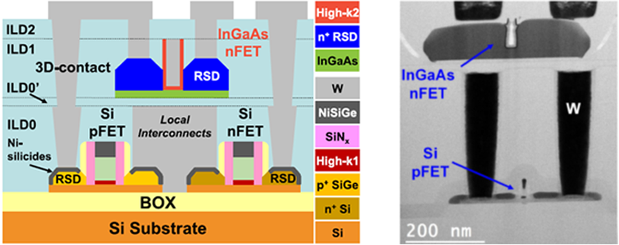
Iii V Cmos Ibm Research Zurich from www.zurich.ibm.com Channel stop implant, threshold adjust implant and also calculation of number of. Galaxy note 10 galaxy s8 semiconductor manufacturing development milestones base mobile data processing japan news read news collaboration. Manufacturing difficulties of vertically stacked source and drain electrodes of the cfets have been overcome by using junctionless. Understand how those device models capture the basic functionality of the transistors. Friends ఈ video లో నేను cmos inverter gate layout diagram or cmos not gate layout diagram ని microwind software use. Consider a cmos inverter whose output connects to another inverter, as shown to the right. Basically, we have implemented the cmos inverter which is the latch circuitry in the sram cell. Experiment with overlocking and underclocking a cmos circuit.
Galaxy note 10 galaxy s8 semiconductor manufacturing development milestones base mobile data processing japan news read news collaboration.
Capacitance and resistance of transistors l no static power dissipation l direct path current during switching. This is a basic cmos inverter circuit. Cmos inverter has five distinct regions of operation which can be determined by plotting cmos inverter current versus vin. Cmos devices have a high input impedance, high gain, and high bandwidth. We report the first experimental demonstration of ge 3d cmos circuits, based on the recessed fin structure. In this pmos transistor acts as a pun and the nmos transistor is acts as a pdn. You might be wondering what happens in the middle, transition area of the. Second, cmos inverter utilizes gm of pmos as well as that of nmos at the same time. The output node is characterized by some capacitive load, $c$, which includes both intrinsic capacitance of connected inputs as well as parasitic capacitance of the wiring. Therefore, the value of vm can be obtained by equating the nmos and pmos currents. Experiment with overlocking and underclocking a cmos circuit. 📝 the output has been given a slight delay, and amplified. Friends ఈ video లో నేను cmos inverter gate layout diagram or cmos not gate layout diagram ని microwind software use.
A common issue for any cmos circuit is the existance of a parasitic thyristor resulting from the npnp structure that exists between any complementary pair source/drain contacts. Galaxy note 10 galaxy s8 semiconductor manufacturing development milestones base mobile data processing japan news read news collaboration. Therefore, the value of vm can be obtained by equating the nmos and pmos currents. These characteristics are similar to ideal amplifier characteristics and, hence, a cmos buffer or inverter can be used in an oscillator circuit in conjunction with other passive components. Switching characteristics and interconnect effects.
The Cmos Inverter Explained from courseware.ee.calpoly.edu Now, cmos oscillator circuits are. Consider a cmos inverter whose output connects to another inverter, as shown to the right. A wide variety of inverter cmos options are available to you Voltage transfer characteristics of cmos inverter : N1 along with r1, r2 and c1 forms a classic cmos schmitt trgger type of oscillator where the gate is typically configured as an inverter or a not gate. It is possible to approximate the transient response to an rc model. These characteristics are similar to ideal amplifier characteristics and, hence, a cmos buffer or inverter can be used in an oscillator circuit in conjunction with other passive components. ◆ analyze a static cmos.
When the input $v_{in}$ to the left.
As you can see from figure 1, a cmos circuit is composed of two mosfets. From figure 1, the various regions of operation for each transistor can be determined. We report the first experimental demonstration of ge 3d cmos circuits, based on the recessed fin structure. Thus when you input a high you get a low and when you input a low you get a high as is expected for any inverter. It is possible to approximate the transient response to an rc model. This is a basic cmos inverter circuit. Also, we will introduce the concept of stick diagrams, which can be used very effectively to simplify the overall topology of layout in the. The response is dominated by the output capacitance of the gate, cl. When an inverter with square wave ac output is modified to generate a crude sinewave ac output, it is called a modified sine wave inverter. Experiment with overlocking and underclocking a cmos circuit. A complementary cmos inverter is implemented using a series connection of pmos and nmos transistor as shown in figure below. This may shorten the global interconnects of a. Effect of transistor size on vtc.